Posts

Showing posts from March, 2011

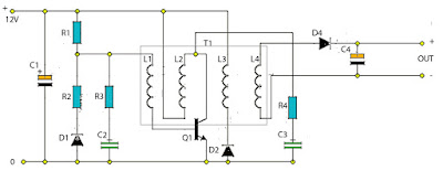
12V to 220V Inverter Schematics

Image
12V to 220V Inverter Circuit Diagrams, Even though today’s electrical appliances are increasingly often self-powered, especially the portable ones you carry around when camping or holidaying in summer, you do still sometimes need a source of 230 V AC - and while we’re about it, why not at a frequency close to that of the mains? As long as the power required from such a source remains relatively low - here we’ve chosen 30 VA - it’s very easy to build an inverter with simple, cheap components that many electronics hobbyists may even already have 12V to 220V Inverter . 12V to 220V Inverter Circuit Diagrams Though it is possible to build a more powerful circuit, the complexity caused by the very heavy currents to be handled on the low-voltage side leads to circuits that would be out of place in this summer issue. Let’s not forget, for example, that just to get a meager 1 amp at 230 VAC , the battery primary side would have to handle more than 20 ADC !. The circuit diagram

Voltage regulator with LT1086

Image
One way to provide good negative-voltage regulation is with a low-drop-out positive-voltage regulator operating from a well-isolated secondary winding of a switch-mode circuit transformer. The technique works with low-dropout types. Under all loading conditions , the minimum voltage difference between the regulator Vin and Vout pins must be at least 1.5V , IC LT1086 low-dropout voltage. If this requirement isn't met, the output falls out of regulation. Two programming resistors, R1 and R2, set the output voltage 12V, and the IC LT1086 servo the voltage between the output and its adjusting terminals to 1.25V. Capacitor C1 improves ripple rejection, and protection diode D1 eliminates common-load problems. Since a secondary winding is galvanically isolated , a regulator 12V output  can be referenced to ground. Therefore , in the case of a negative-voltage output , the positive-voltage terminal of the regulator connects to ground , and the 12V output comes off the anode of D1. The Vin

6V to 220V inverter schematic

Image
Circuit schematic above is one of the voltage inverter circuit , starting from 6-Volt input on the DC current into 220-volt AC output. For maximum output power up to 30W only, and is also very small voltage current. Input voltage plus the entrance on the transistor Q2 to provide the voltage at the collector and then go on Circumference transformer L1 and enter the base. Emitter will be merged ddengan voltage supplied L2 min. And LED 1 is useful as an indicator of whether or not an inverter works especially on the transistor Q2. Part List : R1 = 1K R R2 = 220R C1 = 10nF C2 = 100nF C3 = 47nF C4 = 0,22uF 400V Q1 = 2N5551 Q2 = C5198 LED1 use Green Led Transformer instruction : The above is figure from a place  plastic for copper wire wrapped around, you can also use the marks that have been unused transformer. For the above number are : 1 : Place for copper wire wrapped,with a diameter of 12mm x 10mm. 2 : Hole to place an iron or ferrite rod , with diameter 10mm. 3 : Copper wire that has

Horn siren use the IT and OT transformer

Image
Basically siren on a police patrol car and an ambulance use electronic circuit connected to the DC current. When the switch is pressed, the siren sounds immediately come out. For those of you who own a car, or any motor you can also create a similar horn. Placement was also very practical. And if you want the flashing lights can add your own. In a series of above do not use flashing lights as the sirens sound. Part List : R1 = 47K R2 = 200R C1 = 0,02uF C2 = 50uF 16V C3 = 0,005uF T1 = 2SB178 PNP transistor S1 = Push button switch G1 = 6-12V battery  TR1 , IT transformer is reversed. used a two-legged. TR2 , OT output transformer OT240 How to use it is to put the above series into a box. Adjust the size to be more practical. Then insert the cable of a car or motorcycle battery voltage as described above that is 6-12 V battery into the plug. In accordance with their respective poles. Three feet of IT transformer wrapped so as not to stick to the body of the car or motorcycle. Cover with i

Power supply circuit suitable with high power amplifier

Image
The Power supply circuit suitable with high power amplifier is well designed for large power amplifier circuit and amplifier circuit also requires protection quickly enough so as not to damage because of the power supply is less than the maximum performance or because of a short-circuit on a series of power supply and amplifier. Power supply circuit suitable with high power amplifier is equipped with a fuse, with earth protective chassis. So save on the amplifier and voltage shock to the chassis. In addition to the Power supply circuit suitable with high power amplifier the hum of voices issued almost non-existent because of the high frequency transformer has been issued because of grounded disappeared. In a multichannel amplifier, power supply will fell into one of three types. In order rising costs, and expected decreases the interaction between the channels, namely: 1. Transformer, rectifiers, and reservoir capacitors are shared between channels. 2. Each channel has its own transf

High impedance balance output circuit

Image
Because of high input impedance required to maximize CMRR, High impedance balance output circuit shown in figure below , has been used for the input impedance is determined solely by the input bias resistance R1 and R2. High impedance balance output circuit also useful for interfacing with valve equipment in the strange world of retro-hi-fi. High impedance balance output circuit Adding the output cathode followers for valve circuits are expensive and consume a lot of extra energy, so that the output is often taken directly from the anode gain-stage, as a result, even loading bridge the so-called 10 k distortion can seriously endanger performance and output swing available from the source equipment. All balanced phase dealt with until now have their input impedance is determined by value input resistors, etc., and this can not be raised without lowering the noise performance. High impedance balance output circuit diagrams above shows one answer to this. Input op-amp itself is quite a lo

Versatile and simple power supply

Image
Versatile and simple power supply is one of several series of power supply many other well-known, because making a fairly easy circuit power supply is also nice, versatile addition also can be used on any circuit, for example, Radio tuner, Intregated power amplifier circuit, etc. . But we need to know the Versatile and simple power supply is not used to charge the battery because it will quickly damage the transistors that exist. To have a good output voltage, use of quality components. Versatile and simple power supply Part List : R1 = 1K C1 = 0.22uF 275V C2 = 4700uF 50V C3 = 100n C4 = 220uF C5 = 1000uF Q1 = TIP30 T1 = Step-down Transformer 220V to 12-35V

2 X 0,32W BA5386 amplifier schematic

Image
Amplifier circuit above scheme is a combination of the two IC was then made into one of its supply voltage so it does not require a lot of supply voltage and output a stereo input. Output issued also very low at 2 X 0.32 W and has 8 ohm impedance. Indeed, this amplifier has a very low output, but the amplifier is quite easy to make and does not require much cost. The voltage required at least 4 volts while the maximum supply voltage of 12 volts. Part List : R1,R2______50K trim C1,C2______3u3F C3,C4______100uF C5,C6______470uF U1,U2______BA5386

Headset amplifier via USB

Image
Headset amplifier via USB circuit is a series that is used to add a gain on the headset, which is used on a computer headset. Indeed not only on a computer course in all the headset could also, but in the above circuit voltage to utilize voltage mensupply issued on a PC or laptop via USB. So you need not bother looking for supply voltage, you just take it from USB. Part List : Resistor R1 = 20K R2 = 10K R3 = 10K Capacitor C1 = 3u3F 50V C2 = 100pF Diode D1 = 1N4148 D2 = 1N4148 D3 = 1N4148 D4 = 1N4148 IC U1 = JRC4558 Connector X1 1 = Output 2 = Input 3 = Ground Connector X2 1 = V+ 5V from USB 2 = Ground From USB PCB design Views

2,3 W Mono power amplifier schematic

Image
This amplifier circuit using ic BA534 as a main amplifier, manufactured by ROHM ic, and packaged in SIP1-8. This amplifier circuit has a maximum output of 2.3 Watts with 4 Ohm impedance. Frequency response is between 30Hz to 18KHz. For the voltage needed at least 9 Volt and 13 Volt maximum. For a list of components can be seen below. Part List : R1 = 50K trim R2 = 33K R3 = 68R C1 = 2.2uF C2 = 220uF C3 = 100uF C4 = 47uF C5 = 470uF C6 = 100uF C7 = 47uF C8 = 100n U1 = BA534

Low-cost intregated circuit audio power amplifier

Image
This amplifier circuit is very cheap, because not a lot of components that are required, and the voltage or amperage required is also not too large, so the transformer or power supply is also quite cheap. IC which can be used in power amplifier circuit is the KA2201, LM820M, TBA820M, U820. This amplifier output of 2 W and 4 ohm impedance, which can be applied to the speaker with 4W power, on such small speakers in front of a PC. For the required minimum input voltage of 3 volts and a maximum of 16 volts, for the recommended voltage of 12 volts. Parts Resistor R1 = 100K R2 = 120R R3 = 100R R4 = 10R Capacitor C1 = 0.1uF C2 = 100uF C3 = 47uF C4 = 100uF C5 = 470uF C6 = 220pF C7 = 100nF IC U1 = KA2201 , LM820M, TBA820M, U820

Voltage Doubler with NE555 timer chip

Image
This circuit is used to drives relays of 24 and 18 VDC from a 12 Volt power supply. The basic circuit on the IC NE 555 timer and use this circuit with almost any NPN or PNP power transistor. Parts: Resistor R1 = 47K R2 = 10K R3 = 56R Capacitor C1 = 0.01uF C2 = 0.01uF C3 = 0.001uF C4 = 0.1uF C5 = 50uF Transistor Q1 = TIP29 , TIP120, 2N4922, TIP61, TIP110, or 2N4921 Q2 = TIP30 , TIP125, 2N4919, TIP62, TIP115, or 2N4918 IC U1 = NE555

Intregated Circuit Amplifier with Output Transformer

Image
This amplifier circuit uses the output transformer as an additional amplifier in the output. You can use the transformer output transformer-old has not used but still in good condition, you can use it in this series. For this amplifier IC used is M51503L, this ic has a voltage limit of up to 7 volts only and a minimum of the incoming voltage about 2 volts. Actual output issued from the IC is 0.2 Watts, but once applied to the circuit maximum output of about 5.3 Watts. Part List : Resistor R1 = 75R R2 = 330R Capacitor C1 = 1uF C2 = 47uF C3 = 100uF C4 = 0.33uF C5 = 0.47uF Transformer T1 = Transformer Output OT240 IC IC1 = M51503L

Portable Battery Charger Circuit

Image
This circuit was designed to charge Nicad battery packs in the range of 4.8 to 15.6 V from a convenient remote power source , such as automobile battery. When power is first applied to the circuit applied to the circuit , a small bias current supplied by R1 via winding L1 , starts to turn on the transistor TR1. This forces a voltage across L2 and the positive feedback given by the coupling of L1 and L2 causes the transistor to turn hard on , applying the full supply across L2. The base drive voltage induced across L1 makes the junction the necessary base current to hold Q1 on. Component List Resistor R1 = 1M R2 = 120R R3 = 10R R4 = 39R Capacitor C1 = 100uF 25V C2 = 0.01uF C3 = 4700pF C4 = 100uF 25V Diode D1 = 1N4148 D2 = BYV27-5 D3 = BYV27-5 Transistor Q1 = ZTX650 Transformer L1 = 12T 36awg L2 = 13T 36awg L3 = 20T 30awg L4 = 40T 30awg Core FX3437 with gap of 0.08mm Former DT2492

12 V battery charger with PUT

Image
A short-circuit proof battery charger will provide an average charging current of about 8A to a 12V lead-acid storage battery. The Charger circuit has an additional advantage, it will not function nor will it be damaged by improperly connecting the battery to the circuit. With 220V at the input , the circuit comences to function when the battery is properly attached. The battery provides the current to charge the timing capacitor C1 used in the PUT relaxation oscillator.When C1 charges to the peak point voltage the PUT , the PUT fires turning the SCR on , which in turn applies charging current to the battery. As the battery charges , the battery voltage increases slightly which increases the peak point voltage of the PUT. The voltage on C1 increases until the zener voltage of D1 is reached , which clamps the voltage on C1 , and thus prevents the PUT oscillator from oscillating and charging ceases. The maximum battery voltage is set by potentiometer R2 which sets the peak point firing v

3V to High voltage inverter

Image
Inverter circuit on basic of really taking a series of mosquito racket, a racket in which these mosquitoes require only a low voltage. With only 3 Volts course of this series has been able to work. Circuit is raising the voltage by a transformer that can be made yourself with the need of copper wire and ferrite rods. How to making a transformer like that here , but this circuit requires a step-up transformer that are larger and require a lot of coils. This transformer is controlled by a transistor semiconductor 24D506 in this series. To output issued until 1KV or more but issued is very low amperage. This circuit can also be used in fluorescent lamps 10W maximum . When used in fluorescent lamps add another capacitor to the voltage for provoke can turn on the lights. Part List : Resistor R1____1K5 Ω R2____4K3 Ω R3____22M Ω Capacitor C1____100n C2____100n  400V C3____0.2uF 400V Diode D1___1N4007 D2___1N4007 Transistor Q1___ 24D506 Transformer L1___#100 turns L2___#100 turns L3_

5V 10A output switching power supply

Image
The Schematic above shows a 10A power suplly with a 5V output and with power 50W. It is a flyback converter operating in the continuous mode. The circuit features a primary side and secondary side controller with full protection from fault conditions such as overcurrent. After the fault condition has been removed the power supply will enter the soft start cycle before recomming normal operation. Component Values : Resistor R1_____100Ω R2_____1Ω 1W R3_____10Ω R4_____100KΩ R5_____0.33Ω 1W R6_____10KΩ R7_____390Ω R8_____22KΩ R9_____68Ω R10____10Ω R11____3.3Ω RL_____5Ω 10W Capacitor C1_____0.022uF 400V C2_____470uF  250V C3_____470uF C4_____220pF C5_____470pF C6_____2200pF C7_____270pF C8_____39pF C9_____11,000uF C10____10uF C11____0.047uF Diode D1____1N4937 D2____MBR1035 M1____Diode Bridge Inductor , Transformator L1_____25uH T1_____Lp - 9 mH = 1 : 15 T2_____50 uH. n = 1: 3 Transistor Q1____BUZ80A Q2____GE IRF823

Low Forward Drop Rectifier schematic

Image
A TMOS power FET , Q1 , and LM393 comparator provide a high efficiency rectifier circuit. When Va exceeds Vb1 U1's output becomes high and Q1 conducts. Conversely, when Vb exceeds Va1, the comparator output becomes low and Q1 does not conduct. The Forward drop is determined by Q1's on resistance and current I. The MTH40N05 has an ON resistance of 0.028 Ω ; for I = 10 A , the forward drop is less than 0.3V .Typically , the best Schottky diodes do not even begin conducting below a few hundred mV.

Thermal Controlled battery charger

Image
One way to charge batteries rapidly without abuse is to measure cell temperature and tapper the charge accordingly. The circuit uses a thermocouple for this function. A second thermocouple nulls out the effects of ambient temperature. The temperature difference between the two thermocouples determines the voltage , which appears at the amplifier's positive input. As battery temperature rises, this small negative voltage ( 1 degree Celcius between the thermocouples equals 40uV ) becomes larger. The amplifier, operating at a gain of 4300, gradually reduces the current through the battery to maintain its inputs at balance. The battery charges at a high rate until heating occurs and the circuit then tapers the charge. The values given in the circuit limit the battery-surface temperature rise over ambient to about 5 Degree Celcius. Part List : Resistor R1_____620K R2_____43K R3_____10R R4_____2K R5_____0.6R 5W Capacitor C1_____1uF C2_____0.1uF Diode D1_____1N4148 D2_____1N4001 Transisto

Amplifier simple , easy , and cheap with IC TA7368P

Image
Indeed , this amplifier is suitable known as the title above. Viewed from the schematic alreaady seen that this amplifier circuit requires little components and parts were cheap. This amplifier requires 1 piece of IC TA7368P is manufactered by TOSHIBA is the price too low, then in addition to IC amplifier requires 3 components elco capacitor whose value is not too big. Maybe if you make this amplifier circuit, the total price of all must not be more than $ 1. This amplifier only has more than 1W output, perhaps because it has little strengthening it so that the output is released is very small. But to make this is quite easy and not too costly. Part List : Capacitor C1 = 100 uF C2 = 100uF C3 = 470uF IC IC1 = TA7368P Good Luck :)

Power amplifier for FM radio receiver

Image
Schematic  is suitable for use in radio tuner or FM radio receiver when it is assembled and ready for use. Where if the low gear power radio receiver, with the aid of power amplifier is less powerfull voice / hard to better and just right. For use hios  speakers , use a low-power , because power amplifier has only the power output of 2 X 5 Watt stereo power amplifeir with impedance of 4 Ohm. Working on a minimum voltage of 4.5 Volts and maximum of 16Volt. Use the correct voltage supply - really have been filtered out in order to improve the performance of these power amplifiers. Component Description : Resistor R1________180R R2________180R R3________18K R4________18K Capacitor C1________47uF C2________4.7uF C4________100uF C5________100uF C6________47uF C7________4.7uF C8________47uF C9________100uF C10_______100uF C11_______1000uF C12_______1000uF C13_______100pF C14_______100pF C15_______68n C16_______68n IC IC1_______TA7215P

LM390 power amplifier schematic

Image
Circuit schematic above is / include power amplifiers that have low power output. 1 Watt output power is only based on the IC , and ic used LM390 , manufactered by NS and ic packaged in DIP-14. For output impedance have 4 OHm. Requires a minimum voltage 4 Volt and Maximum voltage is only 9Volt. Part List : Resistor R1________33K R2________510R R3________510R R4________2.7R Capacitor C1________100uF 16V C2________100uF 16V C3________10uF   16V C4________220uF 35V C5________10uF   16V C6________100n IC IC1_______LM390  

3 Watt power amplifier schematic

Image
This time I will share a circuit of schematis power amplifier with LM380 IC that has similarities with LM384. Enough with just a few components you have to make this power amplifier circuit . All components with relatively low prices and making a fairly easy. For this amplifier output power has 3W with 4 ohm impedance. Indeed , this amplifier has the output is quite low and certainly will not be maximal if it works on the speakers with high power. Component List : Resistor R1______________47K R2______________2.7R 2W Capacitor C1______________10uF C2______________470uF C3______________100n C4______________100n IC IC1_____________LM380 , LM384

6 Watt stereo power amplifier schematic

Image
Basiccally,this amplifier works with the IC, which is where ic is associated with several other components in the supply and use DC voltage, which corresponds to the needs of IC above course on the circuit schematic. For IC , stands intregated circuit used is ic LM379 which has a maximum 6 Watt stereo output. This IC manufactered by NS and with SDIP-14 package. While other components needed in the circuit schematic , you can see components of the list below. Component List : Resistor R1___________________2K R2___________________2K R3___________________33K R4___________________33K R5___________________1M R6___________________1M R7___________________10R 2W R8___________________10R 2W Capacitor C1___________________4.7uF C2___________________4.7uF C3___________________470uF C4___________________470uF C5___________________470uF C6___________________100n C7___________________100n IC IC1___________________LM379

LM377 Power amplifier schematic

Image
Various needs of the amplifiers are all different. Different places and use also requires a different power amplifier as well. For this time i gave a circuit schematic power amplifier based on LM377 ic that has similarities with the LM378 and LM1877. Power is smoothly small ouput is 2 X 2.5 Watt and the impedance 4 ohms. Use of this amplifier suitable for portable radio tuner that can be taken every where. Component description : Resistor R1___________________2K R2___________________2K R3___________________1M R4___________________1M Capacitor C1___________________4.7uF 50V C2___________________4.7uF 50V C3___________________100n C4___________________100n C5___________________470uF 50V C6___________________470uF 50V IC IC1__________________LM377 , LM378 , LM1877

Capacitor leakage circuit tester

Image
Generally capacitor that complement with television circuit is often leaked. Consequently spots more rugged display disturbing images running. This is not desired by the owner is not it? For those who know about electronics is certainly a problem. They will find the cause and trying to fix it. For it is not uncommon to use multitester a a search tool damage. But for those who do not have a tool that becomes an obstacle . However , for those of you who enetered last category do not sad because they can assemble their own tester. This tool is very simple but very sensitive to the leackage of a capacitor. Schematic Part List Resistor R1____________________________3K3 R2____________________________100K R3____________________________100K Capacitor C1____________________________10uF 150V C2____________________________10uF 150V Diode D1____________________________K-200 D2____________________________K-200 Lamp__________________________Fluorescent Lamp Switch_________________________On/Off How

FM Radio Transmitter schematic with pcb

Image
For those of you like / love to talk in the air can assemble this simple circuit that can be received by the radio receiver to within a few hundred feet. The voice that issues by this circuit at all clear without rustling. Can also be used to link communications over the air using this radio transmitter, provided that other person also had the same circuit. This PCB design : Description : Resistor R1__________________1K R2__________________18K R3__________________82K R4__________________1K2 R5__________________5K6 R6__________________39K R7__________________18K R8__________________68K R9__________________470R R10_________________100R R11_________________50K XTal Q1__________________ Crystal according to the desired frequency Inductor L1__________________10uH Capacitor C1__________________10uF C2__________________30uF C3__________________20uF C4__________________47uF Transistor Tr1_________________2SB175 Tr2_________________2SB175 Tr3_________________2SB178 Antenna X1-1________________

50W Class-B power amplifier circuit

Image
Power amplifier Class-B is the most popular operating modes, and possibly more than 99% of the current series of power amplifier designed and manufactered are of this class. Defining the Class-B is the amount of bias voltage that causes conduction of both output devices to overlap with the current and thus produce the minimum amount possible crossover distrosi. This Class-B power amplifier performance : Power Output________________________50W RL Impedance_______________________8R Distortion__________________________Below 0.0006% at 1 kHz and 50W/8R Slew rate___________________________Approximately 35V/us Noise______________________________-91dBu at the output EIN_______________________________-117dBu (referred to input) Frequency response__________________+0, -0.5dB over 20Hz-20kHz Part List : Resistor R1,R8____________________________10K R2,R3,R13________________________100R R4_______________________________150R R5,R10___________________________1K R6,R7____________________________68R

1500 Watt high power amplifier

Image
Regarding the 1500 Watt high power amplifier is very nice to talk about single amplifier circuit is therefore not o be outdone by the class-A amplifiers. Power amplifier circuit that allows for use on large event that requires a variety of power or power from the amplifier. In reinforcement in block buffer and its driver transistors using high quality, but actually at the end of the transistor amplifier can be dtermined according to needs. 1500 Watt high power amplifier Component List : R1,R8____________________10K R2,R3____________________22R R4_______________________150R R6,R7____________________68R R9_______________________500R R10______________________1K R11,R15__________________200R R13,R38__________________100R R14______________________15R R16,R17__________________0,22R 2W R18,R19__________________10R 5W R21,R22__________________10K PR1______________________1K C1_______________________10uF 63V C2_______________________220uF 63V C3_______________________100p C6___________________

Radio station blocker circuit

Image
This device is reversal of a radio station , because it sends an empty signal to the frequency chosen in order to remove the actual broadcast. Removing broadcasting? Is the radio transmitter would be lost 10.000W , yes we only use this circuit at close range only , because the utility block radio station not far away . This device needs to close to the antenna radio receiver, at least according to the ammount of radio frequency ( RF ). To the circuit schematic can be see below.  Description : R1____39K R2____10K C1____0.001uF C2____10pF C3____10pF C4____22pF Q1____2N3563 L1____6 turns on ferrite core This is example coil winding : Ferrite diameter 5-8 mm Wire diameter 0.8 mm 6 turns on ferrite. How to use : After the circuit finshed and ready to use , then turn on the device , place tnear a radio receiver that you want. To adjust your signal live racing up and down winding on ferrite which have benen installed. After a suitable signal , the signal received by the radio receiver in the

Long range FM voice Transmitter circuit

Image
This circuit shows how to build a super-sensitive, mini-powered FM transmitter consisting of a RF (radio Frequency) oscillator section interfaced with a high sensitivity, wide pass-band audio amplifier and capacitance mike with a built-in FET (Field Effect Transistor) that modulates the base of the RF oscillator transistor. Transistor Q1 forms a relatively stable RF oscillator whose frequency and is determined by the value of coil L1 and turning capacitor C4. Part List : R1_______15K R2_______3K9 R3_______220R R4,R5____1K R6,R9____10K R7_______390K C1,C6____0.01uF C2_______4.7pF C3_______0.1uF C4_______6-35pf trimmer cap C5_______2.2uF B1_______3V L1_______Coil winding (see below) Q1,Q2____PN2222 M1_______Special FET bypassed microphone Assemble L1 : Form L1 by tightly wrapping eight turns of #16 bus wire on a #8 wood screw. Produces an eight-turn coil with an inner diameter of approximately 0.135 inches and lenght of about 0.625 inches. Insert in the proper hole and solder as shown.

Fan control temperature using sensor LM35

Image
Basic circuit of the LM35 are made to control the fan is either used on amplifier that requires automatic cooling. Its use on power amplifier circuit above and only requires DC fan. From basic sensors based on ic and amplifier op-amp is added again to the transistor Q1 to drive the fan. Part List : R1___220K R2___100K R3___3K3 R4___22K R5___1M R6___150R R7___2K2 R8___33R 4W C1___100pF D1___1N4148 IC1__7915 IC2__TL072 IC3__LM35 F1___DC Fan 12V

Basic LM35 temperature sensor circuit

Image
 This is basic of workmaship LM35 temperatur sensor, whish is taken from the LM35 spending and boosted again by the amplifier op-amp. High output if the sensor is received by ic LM35 high temperature . You can use the output as driver relay, fan , or other. And if yo want to see modifications LM35 temperature sensor see here.  

Temperature protection using PTC and LM393

Image
 Used as a protective circuit above uses a component named PTC , the components in the operating obstacles , but obstacles desert PTC component is influenced by temperature, whereby if the cold temperatures of less than 100 degrees celcius , then this component has a few obstacles. And when temperature run to 100 degrees celcius or higher, which is owned PTC resistance will rise ass well. Because it depends on ambitient temperature , the PTC can be assembled into a circuit protection if high ambitient temperature, tand automatically switchess off, circuit like a schematic above. Part List : R1___4K7 R2___10K R3___1K9 R4___1M R5___4k7 TH1__PTC thermistor IC____LM393

Fan stopped when no audio input

Image
Circuit which is also equipped with temperature sensors would protect the high temperature. However, in the above circuit which necessiatated the input of the amplifier / audio signal. The way it works is , if the amplifier circuit to work and ouput signal to be connected to this circuit , Fan 12V will work well. If the received audio signal this circuit does not exist , then the fan 12V die. And automatic circuit amplifier also not work and does not require refrigeration. Part List : R1_________________220K R2,R9,R10,12,13_____100K R3_________________2K4 R4_________________22K R5_________________1M R6_________________150R R7_________________2K2 R8_________________33R 4W R11________________10K C1_________________100pF C2_________________47uF 25V C3_________________100uF 25V D1,D2______________1N4148 Q1_________________MJE350 Q2_________________MPSA42 IC1________________7915 IC2________________LM35 F1_________________Fan 12 Volt

Combine stereo input to one output

Image
Here , I will give a circuit of schemes that are used to combine 2 pieces input or stereo to 1 input mono. Why 2 inputs in to one because, if we need a stereo amplifier we want to become a stronger by combining the two input into one input, so that a higher power output. Actually without any circuit above we can combine stereo amplifier into mono, but the sound output less than the maximum , need for this additional combiner circuit. Part List = R1______150K R2______920R R3______150K R4______920R R5______920R U1______NE5532 For balance _: R1 / R2=R3 / R4 For balance _: R1 = R3 Gain ______: R5 / R1 = R5 / R3

Addition variable gain amplifier

Image
Variable gain above is a circuit that is used to increase signal strength in dB , needed in a circuit of gains if the range is less reinforcement amplifier input signal, and the required input signal must be high enough so that the circuit is less then the maximum amplifier sound output. For the use of gain can be placed and connected directly to the input amplifier. Part List : R1___15K R2___4K7 R3___15K R4___4K7 R5___180R R6___2K RV1__10K Trim U1___NE5532

Low-Noise operational amplifier.

Image
Low noise balanced input is can also call for the circuit schematic above , because it has a very small noise output and balanced on each input . The noise output is only  117.0 dBu, its very small maybe even not at all out noise. The schematic based on IC5532 , to maintain ic remain good and avoid damage, you should install heatsink in every IC. If the circuit is finished and ready to use, then connect circuit in final befor going out to other components . Because this circuit is also suitable as a buffer amplifier.

High-pass and low-pass filters

Image
Subsonic and ultrasonic filters can be combined into a single circuit for more stable and orderly bandwith. This good and qualified for only two frequencies with the rotation of widely separate. Circuit schematic above shows the rotation of the scond-order or high-pass Butterworth filter in combination with secon-order low-pass filter. Part List : R1___1K R2___1K R3___12K R4___24K C1___4n4 C2___2n2 C3___470nF C4___470nF IC___IC op-amp For the capacitor , use the ceramic capacitors .

Rapid battery charger schematic

Image
The First ac voltage from tranformator will be rectified and filtered to the LM723 voltage regulator and the NPN pass transistors setup for constant current supply. The 470 Ohm resistor is limit trickle current the momentary pushbutton (S2) is depressed, the SCR turn  on , and the current flows through previously determined resistor  network.SCR will be turn off if thermal cutout inside the battery pack opens up.