Posts

Showing posts from February, 2011

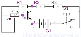
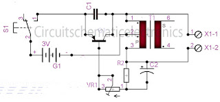
Transistor checker tool with circuit

Image
The above sequence is a circuit of development of the transistor circuit tester before, which of course added few more components , and resulting in even be better. Examiners transistor circuit above only knows his gain is only on the collector . In addition to well known techniques of data materials used therein . That is , if the elements germanium and the like which are in the tool is still functioning or vice versa. Part List : R1=330R/0,5W R2=27K R3=1K R4=1K R5,R6=5K6 C1=1uF C2=2,2uF Q1=Socket transistor T1=Transformator output (OT) S1=Switches friction G1=3V X1-1, X1-2=Speaker connector How to test : Emitter associated with foot condensator and resistor R4, Base is connected with one leg transformer OT , The Collector is connected to the foot of R2 and R3. If you hear a hiss , the sound in few seconds it still has not changed means that transistor still disqualify technical data.

Transistor quality checker

Image
Transistor are the components that have never missed on any electronic circuit . To determine whether the quality is still good or is damaged then need for testing of the transistor . This test is needed before it is installed in an electronic circuit to avoid disappointing results in the future. Thus , all transistors are mounted has been declared unsuitable for use . Please note that th e damage was not located from the transistors can not stand the temperature is too hot . Therefore emphasized here for use tongs as a heat barrier when soldering each feet transistor. Part List : R1=47R R2=100R R3=Resistor with adjustable  to the current Vr1=10K trim Q1=Transistor socket S1=Saklar on/off G1=3V battery To facilitate testing , the provided holes for the third feet on the transistor Q1. At thefoot of the emitter is connected to the battery (+). Base associated with Vr1, and the collectors associated with R2. The voltage (-) that enter the R3 give ampMeter to check quality of the transist

Radio signal interference detector circuit

Image
This circuit is  good for finding component causing incidence trouble voice at radio-set of receiver. Have been realized that in this time a lot of radiation of broadcaster which cannot be arrested by radio receiver limpidly. Sometime - sometime original voice lose to be swallowed  trouble - other voice trouble . So long as in installation each every real correct component, circuit will function properly . Besides can be used for look for the source of voice trouble . This appliance can be made to look for trouble at radio receiver which  not sound at all . Part List : R1=220K R2=4K7 Vr1=100K Vr1=100K C1=10pF C2=1uF C3=1uF L1=100R D1=OA70 Q1=BC327 Q2=TIP42C S1=Switch On/of G1=6V battery Tp=Test Pad SP=Speaker connector To determine the level of interference , then the required injector which is connected with one leg and foot trimpot polar + diode crystal. To be more easier then made the switch as circuit above, the switch is derived from the meeting  trimpot legs that are associated

Fish caller electronics circuit

Image
For those of you who like fishing, this circuit is very suitable for you implement, because it can call the fish and collect a lot of fish so it is easy to provocation and get a lot of fish. Vibrations are excluded from this circuit reaches a distance of several meters in a circle. You can use the river, of where many fish that are easy to find except at sea the waves are fast , so this circuit will not work because it lost by the waves of the sea .Actually , can also be used at sea was calm but the water should not be too choppy. Part List: C1   = 10nF C2   = 47uF/16V VR1= 5K R2   = 470R S1    = Switch On/off Q1   = BC160 T1   = Transformator Output (OT) G1  = 3V battery How to use  the Fish caller circuit : Ater the circuit is finished and sounds biased, then put inside the bottle and sealed for later when inserted in the water is not damged. After the circuit was put into bottles and then put into water, wait several seconds after the switch on/off button. After this circuit

Booster amplifier circuit

Image
The above circuit is a circuit of booster amplifiers or amplifier end of a power amplifier circuit, Circuit over in the most important influence whether or not , and many more are affected in this final series.  Because the booster circuit is the amplifier end of the work was too heavy components causing the rapid component of the heat. If we are wrong then consequences will install components that can cause fatal damaged direct component , such us the installation of pin emiter, collector , and base everything must be correct. In the circuit above can strengthen booster amplifier with maximum work and everything is evenly split, what is it evenly split ? evenly split the point here is that all components can work with the same voltage and the heat evenly , this is because at each respetive base transistor were given the same constrains and same wattage resistor. And to maintain if the power output is too large then the resistor on Re will hamper so that the transistor is not easily br

78XX and 79XX stabilizer circuit with mini PCB design

Image
Here I present the stabilizer circuit of the IC 78XX and 79XX commonly used for voltage stabilization with a mini PCB design , and practical. In the picture above is looking from top the PCB, with a width of 2 cm and 5 cm height. For input voltage can be directly through the AC because i've put it four rectifier diodes are then forwarded to the Elco and IC , that has a stable output in accordance with IC series. What if the IC series 7805 and 7905 , the output voltage of 5 Volts. If the series IC 7812 and 7912 then the output voltage of 12 volts , and so on. See circuit schematic below : Part List : D1,D2,D3,D4 = 1N4007 C1,C2             = 1000 uF/50V C3,C4             = 470 uF/50V IC1                 = 78xx series IC2                 = 79xx series And this is PCB design look from bottom :   PCB design by SIGMA4-Madiun

USB to phone battery charger circuit

Image
Without any   USB to phone battery charger circuit we can charging phone battery using port on USB computer , but it will quickly damage the phone battery, and the battery will bulge. Because the voltage which was issued on usb is 5 volts , while the average-voltage phone battery 3.5 - 3.7 volts. That's why this USB to phone battery charger circuit is required , this USB to phone battery charger circuit reduce votlage to 3.7 volt usb, but will not reduce currents and  will make a durable phone battery . USB to phone battery charger circuit diagrams List of components : R1 : 1 K R2 : 330 R R3 : 4K7 R4 : 300 R R5 : 27R D1 : 4.7 volt zener /1W C1 : 100uF/16V Q1 : BC548 Q2 : BC558A LED1 : Green Led X1-1   : Vcc USB X1-4   : Ground USB X2-1 , X2-2 : To phone battery See also this printed circuit board ( PCB ) of USB to phone battery charger : USB to phone battery charger printed circuit board

Phone Battery Charger circuit

Image
The circuit above is a simple circuit to charge phone battery . Charge battery uses an output transformer secondary voltage fast-flowing with 9 Volt 350 mA. First voltage 220/110/120/240 VAC 50/60 Hz , will be reduced to 9 volts, then rectified by 4 diodes 1N4007 and then flowed to light Led voltage power resistor 1 kOhms inhibited. + directly to the battery volltage and voltage - across 47 Ohm resistor and Led charge indicator which is inhibited resistor 100 Ohm then directly to the phone battery.

-15 Volt output regulated power supply circuit

Image
The circuit above get from -20 volt DC the rectifier diode which is fed to the collector of the Darling pn pass transistor , a TIP105 . The diode use IN4007. The base drive to the TIP105 is supplied through resistor R5. The base of the TIP105 is driven from Vz terminal at pin 9 , which is the anode of a 6.2 -V zener diode that connects to the emitter of the uA723 output control transistor. The method of providing the positive feedback required for foldback action is shown. This technique introduces positive feedback by increased current flow through resistor R1 and R2 under short circuit conditions. This forward biases the base emitter junction of the 2N2907 sensing transistor , which reduces base drive to the TIP105.

+15 V output regulated power supply circuit with uA723 and 2N3055

Image
The supply receive from 220 /120/110 Volt AC , then lowered by the transformer . Then receives +20 Volts DC from rectifier / filter section. This applied to pin 11 and 12 of the IC uA723/LM723 , as well as to the collector of the 2N3055 series pass transistor. The output through R1 and R2, providing about 7 V with respect to ground at pin 4. The reference terminal at pin 6 is tied directly to pin 5 , the non inverting input of the error amplifier . For fine trimming the output voltage , a potentiometer can be installed between R1 and R2. A 100-pF capacitor from pin 13 to pin 4 furnishes gain compensation for the amplifier. Base drive to the 2N3055 pass transistor is furnishes by pin of the uA723. Since desired output of the supply is 1 Ampere, maximum current limit is set to 1,5 Ampere by resistor Rsc whose value is 0,422 Ohm. A 100uF electrolytic capacitor is used for ripple voltage reduction at the output. A 1 kOhm output resistor provides stability for the power supply under no - lo

Dual Tracking regulator circuit

Image
A IC MAX634 inverting regulator is combined with a IC MAX630 to provide a dual tracking approximately 15 Volt output from a 12 Volt DC battery. The reference for the - 15 Volt output is derived from the positive output via R3 and R4. Both regulators are set to maximize output power at low battery voltages by reducing the oscillator frequency , via LBR, when V Batt falls to 8,5 volt. Technical instruction : Max. Input voltage    : 13 Volt / N/a mA Max. Output voltage :-15 Volt , + 15 volt / 45 mA

Stereo Audio Amplifier with IC TEA2024

Image
 The circuit above is based on IC TEA2024, package IC is SIP2-10 and manufactered by THOMSON. Circuit above can be applied anywhere as long as the speaker must be required , do not use powered speakers, it will make this circuit of hot , especially on the IC. So the use of powered speakers with the power output of this circuit. Technical Information : Minimum voltage : 6 Volts DC Maximum voltage: 18Volts DC Power Output       : 2 x 7 Watts Impedance           : 4 Ohms Currents               : 35 mA

14 Watt car audio amplifier circuit

Image
  Basic operation of this amplifier is on IC TEA2021 , In this circuit minimum require voltage is 4 volts and maximum voltage 25 volts. Power output 14 Watt with 4 Ohm impedance. See this schematic.

Low battery detector circuit

Image
You feel confused to detect wether a battery is low or high, or you want to be notified if the battery and has expired , this circuit can detect if a battery has begun to decrease its strength. Circuit is based on LM4250 IC is able to detect if the battery runs out and will issue a notification signal.

Battery charger circuit

Image
This cahrger based on chargeing voltage 2,4 Volts per cell , in accordance with most manufacterers recomendation. This circuit pulses the battery under with 14.4 Volts ( 6 cells x 2,4 volts per cell) at a rate 120 Hz.

Variable charger circuit

Image
Indeed the accu charger circuit , the voltage required must be in accordance with voltage batteries , such accu 12 volts the the output voltage should not be above 12 volts and 12 volts should not be too down. If it does not comply with the required voltage , it will make the batteries or accu quickly broken. But not to worry to find the right voltage to charge to accu, the voltage control circuit is equipped to facilitate in determining the voltage. Transformer Primary : 33 turns #22 Secondary : 45 turns #22 Core : Ferroxcube 203 F 181.3C3

Unique amplifier circuit schmeatic based on IC TDA7255

Image
This circuit equipped with 2 switches that are useful for loudness and filtering, on SW1 as the loudness , SW2 as a filter. It also equipped with direct  adjust of sound on Potentiometer 10k , but only useful as a master volume. Minimum Voltage  : 8 volts Maximum Voltage : 18 volts Maximum Power   : 2 X 13 Watt stereo Impedance Power  : 4 Ohms

Schematic Power Amplifier with IC TDA7370

Image
Here..... this circuit is stereo power amplifier , based on IC TDA7370, its nice Intregated Power amplifier , He does not have hre slightest sound buzzing , although power amplifiers without additional reinforcement , such as filters , tone control, etc. Voltage                      : 9 to 24 volts Max. Power Output  : 2 x 20 Watts Impedance                : 4 Ohms

TDA7240 / TDA7241 amplifier schematic

Image
On this circuit based at IC TDA7240A , this circuit require minimum voltage 8 volt and maximum voltage 18 volt DC. Max power output 40 Watt with 4 Ohm impedance. this circuit can use to Amplifiy the audio device. See the circuit schematic below :

Low voltage audio amplifier circuit from 0,9 volts

Image
Here i share power amplifier based on IC TDA7236 . This amplifier require minimum voltage 0,9 volt and maximum voltage is 1, 6 volt , its very low voltage amplifier. You can use this amplifier everywhere just with one battery 1,5 volt. Power output 16 mW with 32 ohms impedance. see circut below :

1 W low power audio amplifier circuit

Image
This circuit based on IC TDA7233 or you can use  IC TDA7233D . Minimum supply voltage 1,8 volts  and aximum voltage 15 volts. Power Output 1 Watt with 1 Ohm impedance. This circuit include mute switch, which allows you to the mute sound completely.

1,6 Watt intregated circuit audio amplifier

Image
This Circut based on IC TDA7231 , Minimum voltage require 2 Volts and maximum voltage 15 volts . I recomended voltage is 12 volt DC. Power output 1,6 Watt with 4 Ohm impedance. See audio amplifier with IC TDA7231 below :

Tone control mono circuit with C828 / C945

Image
This is mono circuit tone control , include adjusting bass , trebel , and master volume. Minimum voltage require 15 volt and maximum voltage 45 volts.See schematic and construction below :

Master mixer circuit with one potentiometer

Image
This circuit is used for controlling the volume of output  and then entered the mixer, but this circuit not only as the volume setting. This circuit also serves to reduce noise , and increase the gain  at the signal coming from the output. See schematic , PCB line ,and construction below   Master mixer circuit Looked Down Looked Up

600W subwoofer audio amplifier with 20 channel mixer and parametric

Image
This picture below is about my setup subwoofer amplifier with 20 CH mixer and parametric . This amplifier use transformer 10 ampere to supply the power and 3 ampere transformer use to supply mixer and parametric.Elco capacitor that i use for the transformer 10 A, only 10000uF numbered 2. The circuit of amplifiers that i use which is 600 watt mono subwoofer amplifier . And booster amplifier only use 2 Sanken transistors. See picture subwoofer amplifier assemblies below : Looked over the side Front view Back top

1200W power amplifier with sanken

Image
This 1200W power amplifier with sanken using a booster 8 sets sanken , the buffer using transistor D400 and B560 as much 2 sets , and to use part of the driver transistor B546/A940 and D401/C2168 . 1200W power amplifier with sanken have least 20 volts and the voltage to 70 volts maximum with three voltage is +,-,ground. 1200W power amplifier with sanken Power Output 2 X 600 Watt with 8 Ohm Impedance. Circuit audio amplifier 600 Watt Circuit of PCB so from 2  X 600 watts (looked down) Circuit of PCB (looked upon) The above is a circuit of ready to operate , just stay put booster. See also high power amplifier : 2800W High Power Amplifier

Simple Surround audio amplifier circuit based on the IC TDA7053

Image
Perhaps the surround amplifier circuit below is an interesting circuit is made. For, making easy just by using the IC and electrolytic capacitor added 1 , we already can hear the strains of music with sound ( Front Left ,Right and surround Right , Left. In addition to listening to music , this amplifier is also very suitable for gamers who want good sound quality. Minimum voltage requred 9 volts and maximum of 15 volts. Power Output of each speaker 10 Watt with 4 ohm impedance.

1 W mini audio amplifier circuit

Image
In this circuit requires only three components , namely IC TDA7052 , and 2 capacitor electrolyte. Actually , only with IC we are able to run this amplifier , but the sound less than the maximum. This amplifier circuit requires a minimum voltage of 3 volts and 15 volts maximum. Was 1 Watt power output with 4 Ohm impedance. See this circuit below : Just IC and 3 components we can make the circuit above.

Very simple stereo amplifier circuit , with only need 4 components

Image
This is very very simple circuit audio amplifier  based on IC7057T  , you just use 3 components you can make this circuit . And the minimum voltage is 1 Volts , with just 1 Volt  you can operate this amplifier. Maximum voltage 6,5 volts . Maximum Power output 35mW with 32 ohms impedance. See circuit below : Very simple stereo amplifier

Audio power amplifier circuit based on TDA4920 , TDA4925 , TDA4930

Image
Specification : This is stereo amplifier , based on IC TDA4920 , TDA4925 , TDA4930 . Minimum voltage require 9 volts and maximum voltage 13 volts . Maximum power output 2 x 15 Watts with 4 Ohms impedance. Quiescent current 30 mA. See audio circuit scheematic below :

30W , TDA3000 intregated audio amplifier

Image
This circuit based on IC TDA3000 or you can use IC TDA2870 , minimum voltage require 12 volts and maximum voltage require 35 volts DC. Maximum ouput power 30 Watts mono audio amplifier with 4 Ohm impedance. see below the circuit :

Low Power Audio Amplifier Circuit with IC TDA2824S

Image
This is stereo audio amplifier with based on ICTDA2824S , Minimum voltage require 3 volts and maximum voltage 17 volts . Maximum output power 2 X 2 Watt , its low power amplifier. Output impedance  4 ohm. see schematic audio below :

Circuit Battery - Charging Regulator

Image
The Charger Circuits / Circuit Battery - Charging Regulator is capable of charging a 12-Volts battery at up to six ampere rate. Other voltages and currents , from 6 to 600 Volts and up to 300 Ampere , can be accomodated by suitable component selection. When the battery voltage reches its fully charged level , the charging SCR shuts off , and a trickle charge , as determined by the value of R4 , continues to flow. See Circuit Battery - Charging Regulator below : Circuit Battery - Charging Regulator You can use the circuit to charge : Cells battery  Accu wet and dry Rechargeable battery

Charger circuit equipped with a regulator circuit output voltage

Image
The circuit charger is equipped with voltage output settings , so that we can regulate how much voltage to charge the battery. And the settings using the potentio making it easier for us managing voltage up to a mV. See charger circuit below : Adjust the circuit by setting the 500 Ohm resistor while it is attached to a fully charged battery. You can use the circuit to charge : Cells battery Wet Accu Dry Accu Nicad battery Solar battery

Accu charger use a diac and triac

Image
This circuit can be used to charge Accu and cells battery , the circuit can has a very stable output that would make the battery last longer  and maximize the added battery capacity. When charge was also quite fast , so it can optimize the time. A diac is used in the gate circuit to provide a threshold level for firing the triac . C3 and R4 provide a transient suppression network. R1 , R2 , R3 , C1 , and C2 provide a hase - shift network for the signal being applied to the gate. R1 is selected to limit the maximum charging current at full rotation of R2.

Simple Nicad Battery Zapper circuit

Image
This circuit is used to clear the nicad battery internal shorts in nickel - cadmium batteries. To operate this circuit , connect AC cable , then connect a Nicad battery  to the output + , -  and press PB (push button) for three second. See circuit below : Nicad battery zapper